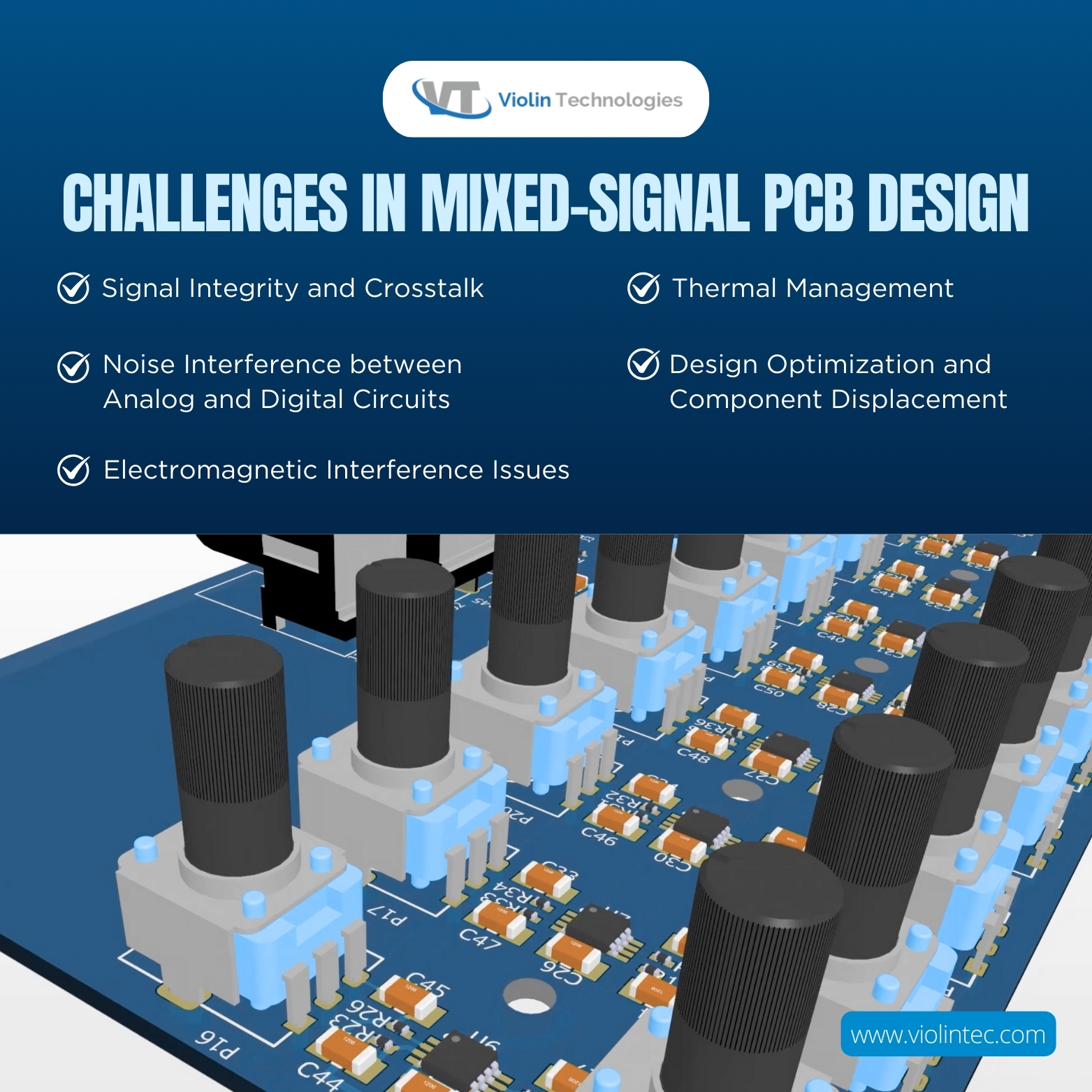
What we cover in this blog?
Understanding Mixed Signal PCB Design
It is pertinent to understand what mixed-signal PCB design entails to grasp all the issues that arise with it. Mixed-signal designs relate to the merging of analog and digital elements into one single printed circuit board. Digital circuits deal with discrete signals, whereas analog circuits process continuous signals. Performance problems may arise when these two signal types coexist because they may interact with one another.
Challenges in mixed-signal PCB design and how to deal with them
1. Signal Integrity and Crosstalk
When digital signals interfere with analog signals, signal integrity problems occur, which can result in data corruption or unpredictable behavior. Crosstalk is the result of adjacent traces’ signals interfering with one another.
Another crippling factor, however, is the fact that digital signals are the noisier ones in comparison to analog digital signals and, as such, pose the greatest threat to sensitive analog signals.
How to Overcome the Issue
- To preserve signal integrity, make sure that the trace width and spacing are constant for controlled impedance traces.
- Ground guard traces should be positioned between important digital and analog signals.
- Utilize differential pairs when routing high-speed signals to minimize interference.
2. Noise Interference between Analog and Digital Circuits
The worst issue for a mixed-signal PCB design is power noise. Many elements contribute to power noise, but the primary culprit lies in digital circuits’ pulse-drawing nature. Such spikes in the current draw will most definitely create fluctuations in the power supply and subsequently cause deep distress for analog circuits. Sensitive analog signals may be distorted or read incorrectly due to high frequency switching noise produced by digital circuits.
How to Overcome the Issue
- Analog and digital components should be physically separated and kept in different areas of the PCB.
- Use ferrite beads or grounded metal shields to block out sources of noise.
- Use low-pass filters to stop analog signals from being impacted by high-frequency noise.
Electromechanical assemblies and box-build manufacturers play a crucial role in delivering complex, customized solutions for various industries.
3. EMI Issues
The close placement of digital and analog circuits is problematic due to the risk of electromagnetic interference (EMI). This is especially true for high-speed digital circuits, which can act as a source of radiation for sensitive analog circuitry.
How to Overcome the Issue
- EMI must be carefully managed, as digital signals can unintentionally radiate into nearby analog traces.
- Routing digital signals with caution is essential to prevent interference with sensitive analog components.
- Shielding using ground planes or enclosures effectively protects analog circuits from high-frequency digital noise.
Contract manufacturers in India play a crucial role in helping businesses scale production while maintaining competitive pricing.

4. Thermal Management in Mixed Signal PCBs
One of the more difficult aspects of PCB design is managing the heat created by components, especially in high-speed and high-power circuits. Excessive heating may damage the components, which in turn leads to failure.
How to Overcome the Issue
- Avoid placing heat-sensitive analog components next to high-power digital integrated circuits.
- Utilize thermal vias and copper pours to effectively dissipate heat, as well as huge copper surfaces.
- Use forced-air cooling or heat sinks for active cooling in high-power applications.
5. Design optimization and Component displacement
Power dissipation from components and their placement are critical to managing the PCB’s thermal efficiency. Component displacement may result in overheating, signal mixing, increased power consumption, or weak heat dissipation. The problem becomes more difficult when trying to maintain balance focused on the intertwining analog and digital circuitry on one board in a mixed-signal PCB design.
How to Overcome the Issue
- Minimize trace lengths for high-speed digital signals to reduce interference and signal loss.
- Isolate sensitive analog components to prevent noise coupling from digital circuitry.
- Ensure sufficient spacing for thermal dissipation and use simulation tools to optimize layout balance.
6. Hardware Debugging
Even with careful planning, hardware issues can arise during the production and testing phases. Debugging a mixed signal PCB often requires specialized knowledge, especially when working with high-speed signals and complex analog components.
How to Overcome the issue
- Use tools like oscilloscopes, signal analyzers, and logic analyzers to diagnose PCB issues effectively.
- Modular testing setups help isolate and test specific components or sections of the circuit.
The Best High-level Assembly Manufacturers can significantly enhance the quality and efficiency of your product’s production process
Conclusion
Mixed-signal PCB design is a complex but challenging task that demands meticulous attention to every detail. From managing signal integrity and power noise to addressing EMI issues and ensuring proper thermal management, each challenge requires its own set of strategies for successful resolution, which include employing the right design techniques, utilizing advanced design tools, and following a well-thought-out routing strategy.
Frequently Asked Questions
What is the primary challenge in mixed-signal PCB design?
The primary challenges in mixed-signal PCB design are managing the interference between analog and digital signals, ensuring signal integrity, and minimizing power noise.
How can I prevent EMI issues in mixed-signal PCB design?
To prevent EMI issues, you should implement a proper routing strategy, use shielding around sensitive circuits, and maintain ground separation between analog and digital sections.
What are the best design tools for mixed-signal PCB design?
Some of the best design tools for mixed-signal PCB design include Altium Designer, Cadence Allegro, and Mentor Graphics PADS, which offer powerful PCB simulation and routing capabilities.
How can contract manufacturers in India help in mixed signal PCB production?
Contract manufacturers in India can provide cost-effective manufacturing solutions for mixed-signal PCBs, offering expertise in high-speed digital and analog circuit fabrication.
