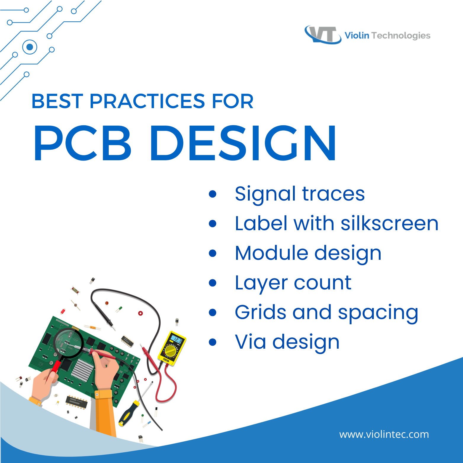
This guide discusses the best practices for achieving top-notch PCB layouts, providing you with the best design software in the manufacturing processes.
Key Takeaways
- Adhere to design principles for optimal PCB performance.
- Prioritize grid spacing and trace length for efficiency.
- Ensure proper power distribution and component grouping.
- Regularly conduct design rule checks and maximize silkscreen usage.
PCB Layout – Learn The Basics
At the core of innumerable electronic devices that we use daily lies a wonder of miniaturization- the Printed Circuit Board (PCB). It is a thin board that contains a network of electronic components.
These surface mount components, such as small resistors and capacitors, are like the building blocks that make the circuit design function. The PCB layout provides a stage for these components to connect and work together, where each component is a unique block.
Essential Components of PCB
1. PCB Board
The bare board is crafted from a non-conductive material like fiberglass or FR4 (a flame-retardant laminate) to ensure electrical isolation between components. This rigid base provides a stable platform for mounting all the other crucial elements.
2. Resistors & Capacitors
- Resistors: Control current flow by providing resistance (measured in ohms), regulating voltage, limiting current, and heat dissipation.
- Capacitors: Act as miniature energy reservoirs, storing and releasing electrical energy to filter noise, stabilize power supply, and provide short-term energy storage.
3. Integrated Circuits (ICs)
Integrated circuits, often called microchips, are the powerhouses of modern PCBs. These miniaturized marvels contain critical components etched onto a single silicon chip. They can perform a vast array of functions, from simple logic operations to processing information in sophisticated devices like smartphones and computers.
Need your product built? Find the perfect contract manufacturers to bring your vision to life.
4. Conductive Tracks and Pads
Think of the conductive tracks and pads as the intricate network of roads and bridges in your PCB city. Pads are small metal power planes where components are soldered onto the printed circuit board traces, creating the essential connections within the circuit.
Different Types of PCBs
The world of PCBs extends beyond a one-size-fits-all approach. Different applications demand PCBs with specific properties, leading to a diverse range of board types. Let’s explore some of the most common:
Single-Sided PCBs
The components are mounted on one side, with a single layer of copper tracks etched on the other. Think of them as the workhorses for simpler electronic devices like power supplies or radios. Their advantage lies in their low cost and straightforward design, making them ideal for applications where space and complexity aren’t major concerns.
Double-Sided PCBs
Double-sided PCBs take things a step further. They boast conductive copper tracks on both sides of the board, significantly increasing the real estate for components and connections. This allows for the creation of more intricate circuits to manage electromagnetic interference, making them suitable for a wider range of devices like calculators and basic controllers.
Multilayer PCBs
For highly complex electronic marvels like smartphones and computers, multilayer PCBs reign supreme. Additional layers of conductive tracks are separated by insulating material.
These PCBs can have anywhere from 4 to 12 layers or even more in advanced designs. Similar to double-sided boards, vias connect the various layers to the power plane, enabling intricate electrical pathways within a compact space. Multilayer PCBs cater to situations where space is a premium and high-performance circuits are needed.
Rigid PCBs
These sturdy PCB layout strengths allow them to support heavier components and are commonly found in desktop computers and other stationary electronics. While robust, their rigid nature limits their use in applications requiring efficient heat dissipation.
Flexible PCBs
These PCBs utilize flexible materials like plastic or Kapton, allowing them to bend and conform without compromising the signal quality. These are ideal for applications like cameras and mobile phones.
The PCB Process
Crafting a functional PCB is a meticulous process with several key steps:
- Schematic Capture: This initial phase designs the component footprint – a schematic diagram – representing the circuit using symbols for each component and its connections. Specialized software streamlines this process.
- Component Placement: Here, the blueprint transforms into reality. Components are meticulously positioned on the PCB, power circuit interference, space constraints, and heat dissipation.
- Routing: Routing involves connecting components with thin copper tracks and establishing the pathways for high-speed signals. Signal integrity, power regulation and distribution, and thermal management are all crucial aspects to consider during this intricate stage.
Thinking of collaborating with the best? Connect with the right electromechanical assembly and box-build manufacturers now.

PCB Design Rules: The Guiding Principles
PCB design rules guarantee a functional and reliable circuit board. These guidelines include:
- Signal Traces: The route traces and trace lengths dictate the size and placement of vertical and horizontal trace routing strategically for proper current flow.
- Label with Silkscreen layer: Silkscreening must be considered while designing traces, component locations, grids, and grouping to guide electron flow. Silkscreening greatly simplifies manufacturing, user function, testing, service, and engineering.
- Module Design & placement: Strategic positioning of ground or power plane considering current carrying capacity and thermal relief pattern for components that generate heat frequently.
- Layer count: The number of PCB layers (single, double, or multilayer boards) significantly impacts functionality and manufacturability.
- Grids and spacing: Maintaining proper spacing between conductive elements prevents electrical arcing and leakage currents. Try to incorporate dedicated power planes for each power supply stage to maintain signal integrity.
- Via design: The size, type, and placement of vias ensure proper connections between signal layer(s). Ensure ground planes are connected to the ground connection for the power supply.
Conclusion
By following best practices for ground plane, routing, and adhering to design rules, a PCB manufacturer can make the manufacturing process hassle-free.
Your PCB design can be brilliant, but flawless execution is key. Violin Technologies translates your vision into reality. We offer efficient electromechanical assembly, rigorous testing, and global supply chain support. Get your perfectly designed PCBs transformed into high-performing devices on time and budget. Contact us now!
Frequently Asked Questions (FAQs)
What are the best practices of PCB layout?
Prioritize short, direct traces for efficient signal flow and minimize EMI.
What are the top 3 important steps in the PCB design and layout process?
Top 3 PCB layout Steps:
- Schematic Capture: Plan the circuit’s blueprint with components and power of ground plane connections.
- Component Placement: Strategically position components for high-speed digital signals and performance.
- Routing: Connect components with copper traces, considering signal integrity and thermal management.
How do you make a good PCB design?
Balance functionality, manufacturability, and quality control process. Follow design rules, prioritize short routing traces, and manage heat effectively.
How do I optimize my PCB layout?
Minimize trace routing length and bends, group components by function, and utilize heat sinks to dissipate heat.

Almaas Saleem
About the Author
Almaas Saleem is a skilled software engineer from Kerala, India who currently resides in East Africa. She is passionate about technology and constantly seeks to learn more about it through reading and hands-on experience. Almaas excels in web development, design, automated testing software, ethical hacking, cybersecurity, and digital marketing. She also works as a technical writer for new businesses, managing various entities. Almaas is distinguished by her steadfastness and commitment to her work, which consistently ion.

